


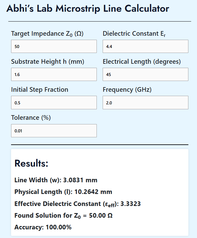
Target Impedance Z0 (Ω) Substrate Height h (mm) Initial Step Fraction Tolerance (%) Dielectric Constant Er Electrical Length (degrees) Frequency (GHz) Explore Other Blog Posts Abhi’s Lab...
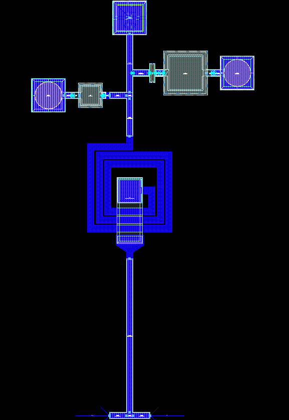
Introduction A bias network is used to supply the necessary DC voltages to the terminals of any amplifier. The main design goals for the bias network are: RF-DC isolation >20 dB RF port return loss...
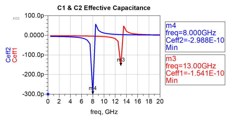
Introduction Capacitors are equally vital in RF and microwave circuits, enabling critical functions like DC blocking, impedance matching, and harmonic filtering. However, their high-frequency...
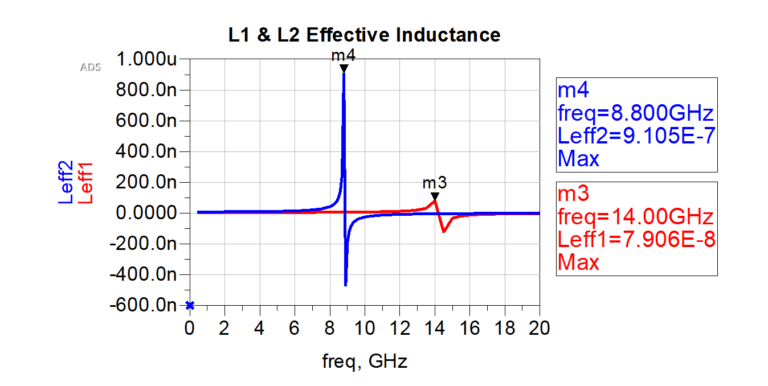
Inductors are indispensable components in RF and microwave circuits, playing crucial roles in filtering, impedance matching, and signal tuning. However, their behavior at high frequencies is far from...