An Overview of Gallium Arsenide (GaAs) MMIC Technology: Principles, Process, and Performance
1. Introduction to GaAs MMIC Technology
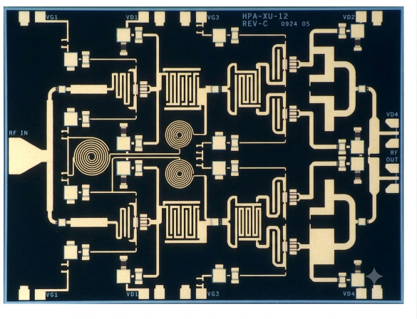
Monolithic Microwave Integrated Circuits (MMICs) integrate active devices (such as transistors) and passive network components (such as inductors, capacitors, and microstrip transmission lines) onto a single semiconductor substrate to operate within the microwave (300 MHz – 30 GHz) and millimeter-wave (30 GHz – 300 GHz) frequency spectrums.
While silicon CMOS remains the dominant technology for digital logic and low-frequency mixed-signal integrated circuits, Gallium Arsenide (GaAs) serves as a core III-V semiconductor material for high-frequency, low-noise, and high-efficiency RF front-end architectures.
“At microwave frequencies, parasitic capacitance and wire-bond inductance present significant impedance matching challenges. GaAs MMICs mitigate these parasitic interconnects by monolithically integrating passive matching circuits alongside active devices.”
Key Material Properties: GaAs vs. Silicon
GaAs offers several intrinsic material advantages over Silicon ($\text{Si}$) for RF and microwave operations:
- Electron Mobility: GaAs exhibits an electron mobility of approximately $8,500 \text{ cm}^2/(\text{V}\cdot\text{s})$ at room temperature, compared to $\sim 1,400 \text{ cm}^2/(\text{V}\cdot\text{s})$ for Silicon.
- Direct Bandgap: With a bandgap $E_g \approx 1.424 \text{ eV}$, GaAs allows efficient high-speed charge transit and optoelectronic integration.
- Semi-Insulating Substrate: GaAs substrates can be grown with resistivities exceeding $10^7 \ \Omega\cdot\text{cm}$, significantly lowering dielectric substrate losses at high frequencies relative to bulk silicon.
2. Active Transistor Architectures
GaAs MMICs primarily leverage two active device topologies depending on power, noise, and frequency requirements:
Pseudomorphic High Electron Mobility Transistor (pHEMT)
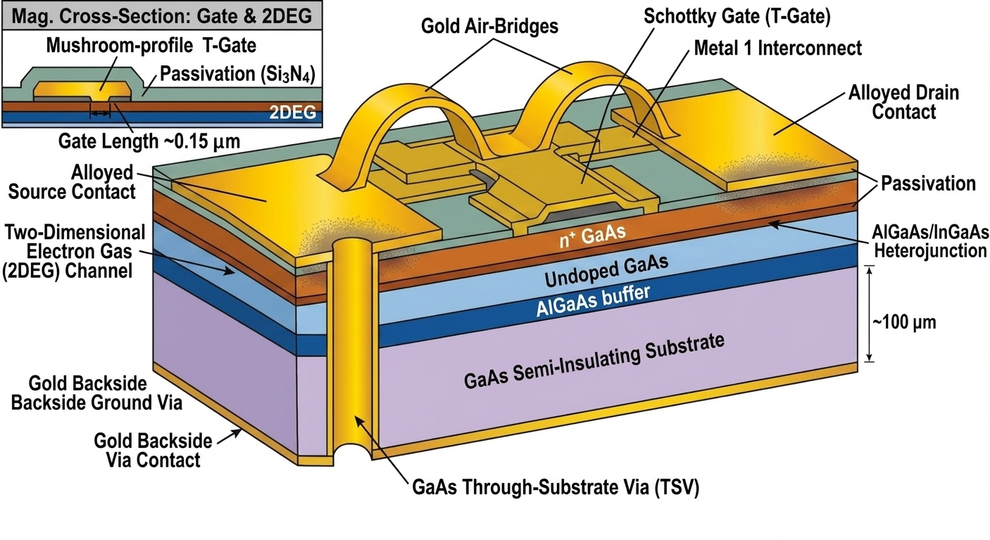
- Utilizes heterojunctions (e.g., $\text{AlGaAs/InGaAs}$) to form a Two-Dimensional Electron Gas (2DEG).
- Characterized by high electron velocity and low noise figures ($NF$).
- Primary Applications: Low-Noise Amplifiers (LNAs), wideband switches, and millimeter-wave mixers up to 100+ GHz.
Heterojunction Bipolar Transistor (HBT)
- Utilizes vertical conduction with high current density per unit area.
- Requires only a single positive power supply and offers low phase noise.
- Primary Applications: High-efficiency Power Amplifiers (PAs) and Voltage-Controlled Oscillators (VCOs).
Feature Comparison Matrix
- Pseudomorphic High Electron Mobility Transistor (pHEMT)
- Heterojunction Bipolar Transistor (HBT)
- Integrated Metal-Insulator-Metal (MIM) capacitors and spiral inductors
- Through-Substrate Vias (TSVs) for low-inductance ground return
- Complementary P-channel devices (GaAs lacks practical high-mobility p-channel FETs)
3. Fabrication & Process Flow
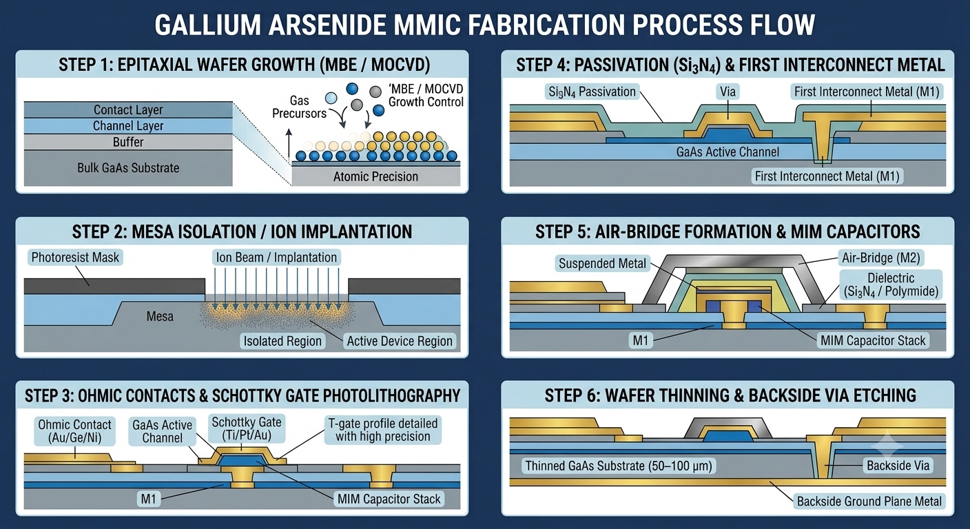
The manufacturing process of a GaAs MMIC integrates front-end wafer fabrication with back-end substrate thinning and via etching:
Wafer Thinning and Backside Vias
Ground continuity at microwave frequencies requires minimal parasitic inductance. GaAs substrates are mechanically thinned to $50 \ \mu\text{m}$ or $100 \ \mu\text{m}$, after which Inductively Coupled Plasma Reactive-Ion Etching (ICP-RIE) forms Through-Substrate Vias (TSVs). Gold plating lines the vias, connecting the front-side source pads directly to the backside ground plane.
4. Mathematical Modeling & Fundamental Equations
Unity Gain Cutoff Frequency ($f_T$)
The unity-current-gain cutoff frequency ($f_T$) of a GaAs pHEMT is determined by transconductance ($g_m$) and gate parasitic capacitances ($C_{gs}$, $C_{gd}$):
$$f_T = \frac{g_m}{2\pi (C_{gs} + C_{gd})} \approx \frac{v_{sat}}{2\pi L_g}$$Where:
- $v_{sat}$ is the electron saturation velocity.
- $L_g$ is the physical gate length.
- For a $0.15 \ \mu\text{m}$ gate length pHEMT, typical cutoff frequencies exceed 90–110 GHz.
Microstrip Characteristic Impedance ($Z_0$)
For a microstrip line of width $W$ on a GaAs substrate of thickness $h$ with relative permittivity $\varepsilon_r \approx 12.9$:
$$Z_0 \approx \frac{120\pi}{\sqrt{\varepsilon_{eff}} \left[ \frac{W}{h} + 1.393 + 0.667 \ln\left(\frac{W}{h} + 1.444\right) \right]}$$5. Technology Comparison
The table below summarizes performance parameters across mainstream semiconductor RF technologies:
| Metric / Parameter | GaAs pHEMT / HBT | GaN HEMT | RF CMOS / SOI | SiGe BiCMOS |
|---|---|---|---|---|
| Max Cutoff Frequency ($f_T$) | High (100–150 GHz) | High (90–140 GHz) | Moderate (<90 GHz) | High (200–300 GHz) |
| Power Density | Medium (~1–2 W/mm) | High (>5–10 W/mm) | Low (~0.2 W/mm) | Low-Medium (~0.5 W/mm) |
| Breakdown Voltage ($V_{BD}$) | ~10–15 V | >50–100 V | ~2–3 V | ~3–5 V |
| Minimum Noise Figure ($NF_{min}$) | Low (<0.5 dB) | Moderate (~1.0 dB) | Fair (~1.5 dB) | Good (~0.8 dB) |
| Substrate Loss | Very Low | Low | High (unless SOI) | Moderate |
| Manufacturing Cost | Moderate | High | Low | Low-Moderate |
6. Design Considerations & Practical Callouts
Design Note: Transmission line lengths for lumped LC matching elements in GaAs MMICs should generally be kept below $\lambda/10$ at the highest harmonic frequency to prevent unwanted transmission line phase delays and distributed effects.
Thermal Management: Gallium Arsenide exhibits a lower thermal conductivity ($\approx 0.46 \ \text{W/cm}\cdot\text{K}$) compared to Silicon ($\approx 1.5 \ \text{W/cm}\cdot\text{K}$) and Silicon Carbide ($\approx 3.7 \ \text{W/cm}\cdot\text{K}$). High-power GaAs HBT arrays require thermal dissipation vias directly beneath active finger regions.
Mechanical Handling: GaAs wafers are more brittle than Silicon wafers due to their crystal structure. Automated handling tools must use regulated vacuum pressure and precise chuck torque to avoid wafer cleavage during processing.
7. Terminology Glossary
- Air-Bridge: A suspended metallic connection formed during front-end processing to cross over underlying signal traces while maintaining air dielectric separation to minimize parasitic capacitance.
- MIM Capacitor: Metal-Insulator-Metal capacitor formed using a thin film of dielectric material (typically Silicon Nitride, $\text{Si}_3\text{N}_4$) between two metal layers.
- PDK (Process Design Kit): A foundry-provided suite of simulation models, DRC (Design Rule Check) files, and layout components used in EDA software (e.g., Keysight ADS, Cadence Virtuoso).
8. Key Takeaways & Applications
- 5G and Satellite Communications: GaAs MMICs remain standard components in sub-6 GHz and mmWave beamforming modules, providing high efficiency in driver and LNA stages.
- Radar Systems: Utilized extensively in X-band and K-band phased-array radar systems for aerospace and defense electronics.
- Complementary Technology Integration: Modern RF front-end architectures often integrate GaAs LNAs alongside high-power GaN output stages.

Verified References & Further Reading
- S. M. Sze and K. K. Ng, Physics of Semiconductor Devices, 3rd ed. Hoboken, NJ: Wiley-Interscience, 2006.
- I. D. Robertson and S. Lucyszyn, Eds., RFIC and MMIC Design and Technology, London, U.K.: The Institution of Engineering and Technology (IET), 2001.
- R. S. Pengelly, S. M. Wood, M. P. Fagerlund, and A. W. Dearn, “Commercial applications of GaAs MMICs,” IEEE Transactions on Microwave Theory and Techniques, vol. 50, no. 3, pp. 1024–1035, Mar. 2002.
- J. A. Higgins, “GaAs FET technology for microwave integrated circuits,” IEEE Transactions on Microwave Theory and Techniques, vol. 26, no. 2, pp. 72–82, Feb. 1978.