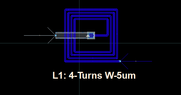
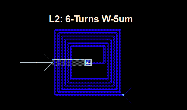
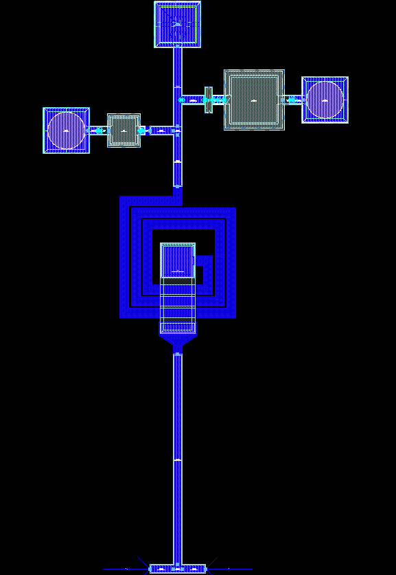
Inductors are indispensable components in RF and microwave circuits, playing crucial roles in filtering, impedance matching, and signal tuning. However, their behavior at high frequencies is far from ideal due to inherent parasitic elements that limit their performance. One key parameter that defines the usable frequency range of an inductor is its self-resonant frequency (SRF) – the point where the inductor’s parasitic capacitance resonates with its inductance, causing it to lose its inductive properties. In this blog, we will explore the concept of SRF, analyze how parasitic elements influence it, and compare two spiral inductors with different geometries to understand the trade-offs involved in high-frequency inductor design.
No inductor is purely inductive. All practical inductors exhibit three parasitic elements that degrade performance at high frequencies:
-
Equivalent Series Resistance (ESR)
-
Arises from the resistive losses in the conductor material (e.g., copper traces) and substrate coupling.
-
Causes power dissipation, reducing Q-factor and efficiency.
-
Equivalent Parallel Capacitance (EPC)
-
Generated by:
-
Inter-winding capacitance between adjacent spiral turns.
-
Substrate capacitance between the inductor and ground plane.
-
Fringing fields at the edges of the metal traces.
-
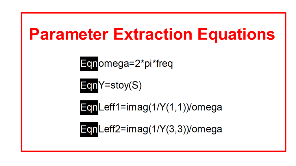
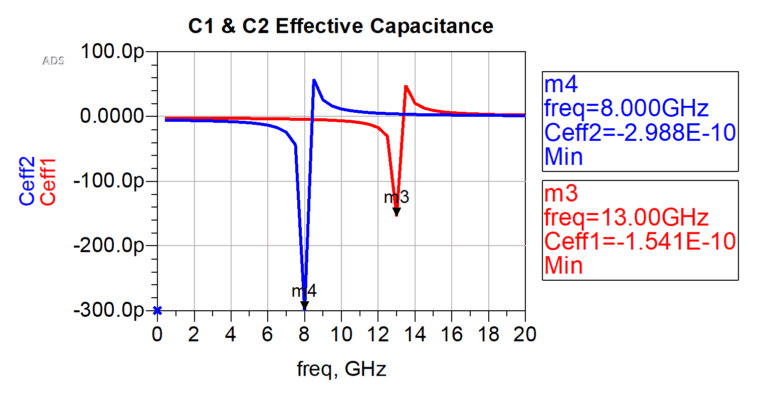
Forms a resonant tank with the inductor’s inductance (L), creating the self-resonant frequency (SRF).
-
Distributed Parasitic Inductance
-
Even non-inductive components (e.g., traces, vias) exhibit unintended inductance due to current flow paths.
-
Affects high-frequency impedance and signal integrity.
-
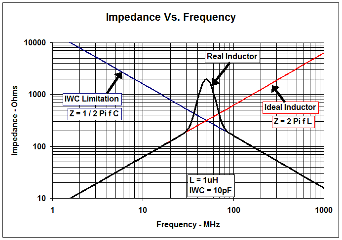
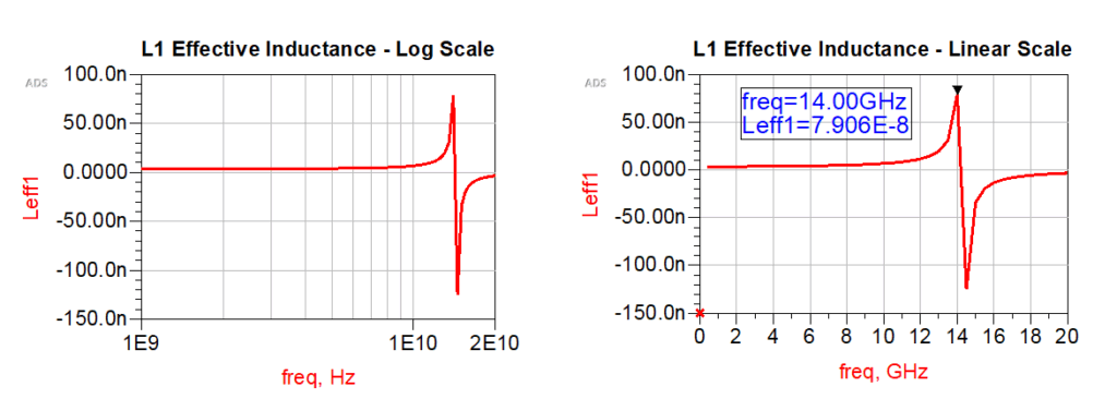
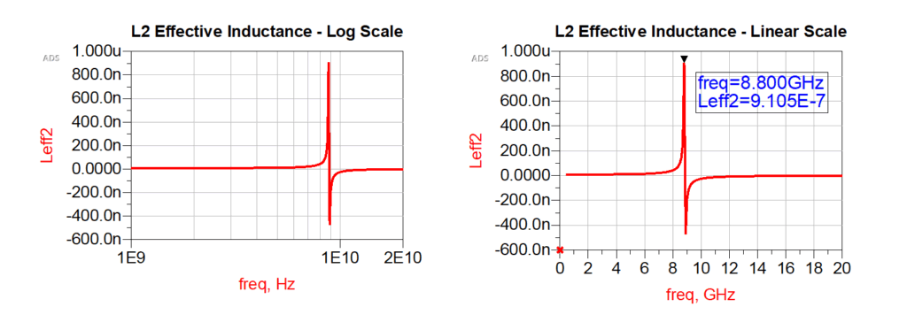
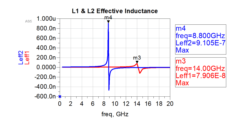
Below SRF: The inductor behaves as intended, with impedance increasing linearly (Z=jωL).
-
At SRF: The impedance peaks (Z→∞), creating an open circuit due to parallel resonance.
-
Above SRF: The parasitic capacitance dominates, turning the inductor capacitive (Z=1/jωCp).
-
Signal Paths: Operate inductors below SRF to avoid nonlinear behavior. For example, a 14 GHz SRF inductor should be used below ~10 GHz.
-
Bias Chokes: Intentionally operate near SRF to maximize impedance for noise rejection.
-
Layout Sensitivity: Substrate thickness and dielectric constant (ϵr) directly influence Cp. Thinner substrates (e.g., GaAs) increase Cp, lowering SRF compared to thicker substrates like alumina